Wednesday, October 25, 2017

Aixtron's sale of ALD/CVD Product Line to Eugene Technology in South Korea gets US approval

Aixtron SE (AIXG), announced Tuesday that the Committee on Foreign Investment in the United States or CFIUS has approved the sale of ALD and CVD memory product line. 
Eugene Technology CEO Eom Pyeong-yong (left) and Aixtron CEO Kim Schindelhauer pose for a photo holding their contract. (Picture credit: Pulse by Maeil Business Newspaper & mk.co.kr LINK)
The company noted that the investigation by the CFIUS of the sale of AIXTRON's ALD and CVD memory product line to Eugene Technology in South Korea resulted in a determination that there are no unresolved U.S. national security concerns from CFIUS' perspective.
Full report: LINK

Monday, October 23, 2017

Picosun’s ALD technology improves lifetime and reliability of electronic circuit boards

ESPOO, Finland, 24th October, 2017 – Picosun Oy, leading provider of advanced Atomic Layer Deposition (ALD) solutions for global industries, has invented an ALD-based method(*) with which the operational lifetime and reliability of printed circuit board assemblies (PCBA) can be efficiently improved.

Metal whisker formation and corrosion are some key factors that cause PCBA performance degradation over time. Metal whiskers are thin filaments or threads growing out from solders, components, and interconnects on the PCBA, and they can cause short-circuiting that leads to a system failure. This is particularly fatal in several sensitive applications such as medical, automotive, space, aviation, military, and industrial control electronics. 
Previously, lead has been added to solder alloys to prevent whisker formation, but the current environmental regulations prohibit its use. This is why novel methods, such as the ALD-based surface protection technique developed and now industrially enabled by Picosun are very much sought after amongst the electronics manufacturers. In Picosun’s approach, application-specifically tailored ALD nanolaminate forms a dense, conformal, and hermetic seal on the PCBA. This seal protects the PCBA components from the corrosion caused by moisture and impurities in the ambient air and blocks the metal whisker propagation. As ultra-thin films, ALD coatings have the additional benefit of allowing postprocessing of the PCBA, and they do not increase its mass or dimensions. Furthermore, as a gas-phased technique, ALD is gentle to the surface, it can be applied at moderate temperatures, and it is environmentally friendly.


“Our PCBA protection technology has gained lots of interest amongst our clients both in industries and in R&D, and many are eager to start applying it in their manufacturing processes. Electronic circuit board industry is a vast, global market, where we are happy to utilize our ALD knowhow to enable products of extended lifetime and improved safety and reliability. Our comprehensive selection of industrial ALD systems guarantees an optimal solution to every customer, allowing fast and economic processing of even large area PCBAs in just one process run,” states Juhana Kostamo, Managing Director of Picosun.
(*) Pat. pending

AMEC Celebrates 100-Chamber Shipment Milestone For Prismo A7 MOCVD System Used To Manufacture LEDs

SHANGHAI, Oct. 23, 2017 /PRNewswire/ -- Marking a milestone for its Metal Organic Chemical Vapor Deposition (MOCVD) business, Advanced Micro-Fabrication Equipment Inc. (AMEC) today announced that it has shipped 100 Prismo A7™ MOCVD tool chambers since the product's introduction last year.  It is AMEC's second-generation MOCVD tool, and is used by customers to manufacture gallium nitride-based (GaN) Light Emitting Diodes (LEDs) for solid-state lighting products, and other applications. Each Prismo A7 system contains up to four chambers. Production throughput is more than twice as high as AMEC's first-generation MOCVD tool, the Prismo D-BLUE. 
 
 
The products are installed at customer facilities in China, where the majority of the world's LED devices are produced. Customers include leading Chinese LED manufacturers, San'an Optoelectronics and HC SemiTek Corporation. Since its introduction, AMEC has received multi-tool orders, as well as repeat orders for the system. Sales momentum is brisk, and by the end of this year, the company expects to record shipments of approximately 120 chambers.


Source: PR Newswire LINK

Thursday, October 19, 2017

ALD FOR INDUSTRY, MARCH 21 – 22, 2018 – DRESDEN

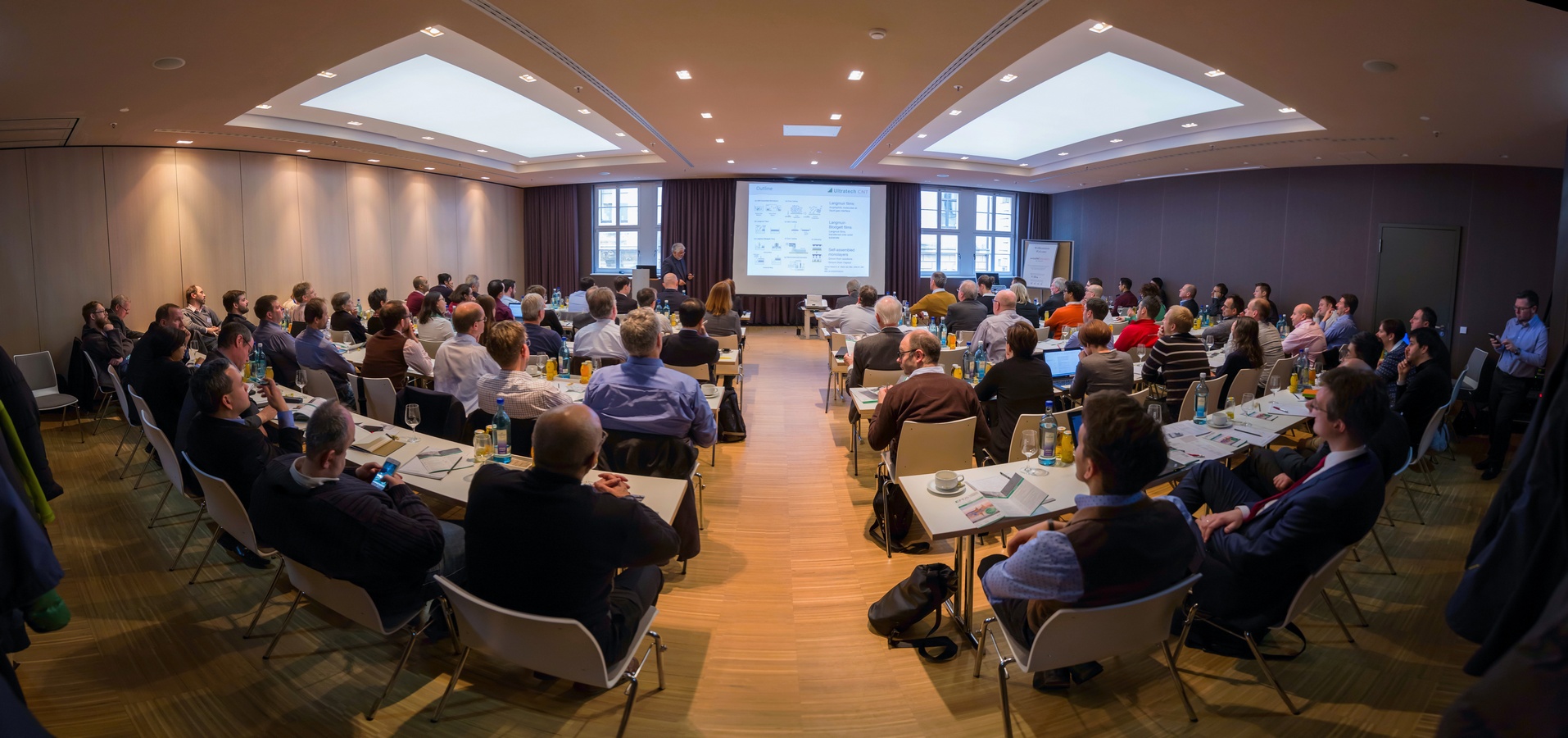
ALD FOR INDUSTRY, MARCH 21 – 22, 2018 – DRESDEN: Following the succes of ALD for Industry 2017 with 100 participants we will continue to organize this event. This time we have extended the Workshop with half a day to a full 2 day event and the ALD Exhhibition will also be open for the public! In addition, the part of the workshop will be a HERALD Event so please contact us for more details on that.

Conference Chairs: Jonas Sundqvist, Fraunhofer IKTS and Christoph Hossbach, Picosun Germany
Tutorial Chair: Colin Georgi, Fraunhofer ENAS

Committee: Bernd Hintze (invited speaker), Globalfoundries and Henry Bernhardt, Infineon


Background: A topical workshop with focus on industrialization and commercialization of ALD for current and emerging markets Atomic Layer Deposition (ALD) is used to deposit ultrathin and highly conformal thin films. ALD is unique in the sense that it employs sequential self-limiting surface reactions for growth in the monolayer thickness regime. 

ALD in Germany: According to market estimates the equipment market alone is currently at an annual revenue of US$ 1.5 - 1.7 billion (2017) and it is expected to double in the next 4- 5 years. In a European context ALD was invented independently twice in Europe (Russia & Finland) and since the last 15 years Germany has grown to become one of the strongest European markets for ALD in R&D, chemicals, equipment and end users. Here, Dresden and Saxony isa unique ALD hotspot due to a strong semiconductor and equipment industry.

The Event will focus on the current markets for ALD, besides the leading edge semiconductor industry, applications in MEMS and Sensors, Display, Lightning, Barriers and Photovoltaics will be addressed.

 
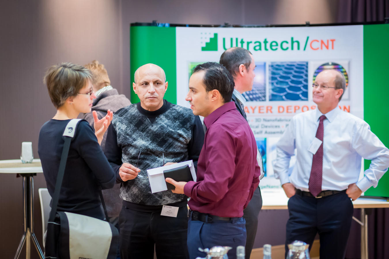
Sponsors (signed so far):

CONTACT:
Dr. Katrin Ferse
Europäische Forschungsgesellschaft Dünne Schichten e. V.
Gostritzer Str. 63, 01217 Dresden, Tel. +49 351 871 8374, Fax: +49 351 8718431
E-Mail: ferse@efds.org, web: www.efds.org
 
Dr. Jonas Sundqvist 

Fraunhofer IKTS, Dünnschicht-Technologien | Thin-Film Technologies, Winterbergstraße 28, 01277 Dresden, Germany
Telefon +49 351 2553 7693, Mobile +49 173 4394 239
E-Mail: jonas.sundqvist@ikts.fraunhofer.de
www.ikts.fraunhofer.de


Tuesday, October 17, 2017

Lam Research Corporation 2018 Q1 - Results - Earnings Call Slides

(Seeking Alpa) Oct. 17, 2017 6:20 PM ET. The following slide deck was published by Lam Research Corporation in conjunction with their 2018 Q1 earnings call.
LINK to slides: here

Veeco Receives First Order for New GENxcel MBE System

Veeco Instruments announced that Acken Optoelectronics will receive the first shipment of Veeco's new GENxcel Molecular Beam Epitaxy (MBE) System.

Acken Optoelectronics Ltd. is a Chinese start-up company specializing in development of high-speed communication devices including advanced optoelectronic communication, RF switching, and low noise amplifiers for mobile applications.

Source: LEDinside LINK

 
Veeco's new GENxcel Molecular Beam Epitaxy (MBE) System (Image from Veeco)

Monday, October 16, 2017

Tokyo Electron & Spin Transfer Technologies signes alliance to bring MRAM to the next level

Spin Transfer Technologies, Inc. (STT) and Tokyo Electron Ltd. (TEL) have today signed an agreement for a collaborative engineering program for next-gen SRAM and DRAM-class ST-MRAM devices.

TEL PVD EXIM have explored its unique capabilities to form multi-layer magnetic tunnel junction (MTJ) stacks for spin-transfer-torque magnetoresistive random access memories (STT-MRAM).

The agreement aims to further the advance of ST-MRAM, a new class of high-performance, persistent memory devices, to provide previously unachievable levels of speed, density, and endurance. The combination of STT’s ST-MRAM technology and TEL’s advanced PVD MRAM deposition tool will allow the companies to quickly develop processes for the highest density and endurance devices. 

Source: Evertiq LINK

Monday, October 2, 2017

NCD signed the large-scale contract to supply ALD equipment to Chinese DMEGC for high efficiency solar cells

NCD has just received the large-scale contract with Chinese DMEGC to supply up to 400MW solar cell manufacturing ALD equipment. This mass production equipment is several Lucida (TM) GS1600 ALD and Automation Systems to produce high efficiency crystalline solar cells with depositing fast high quality Al2O3 ALD on Si wafers. It is repeat order of the same system supplied in the production line in 2016 because the customer has been satisfied with the excellence of the system, that is, NCD’s technology and competitiveness are confirmed by the Chinese customer again. NCD is discussing supply agreements with many other customers besides this contract so is looking forward to rapid sales growth in the near future. 

Sunday, October 1, 2017

TSMC to new build 3nm fab in Taiwan


TSMC said that the company's planned advanced 3nm fab will be located in the Tainan Science Park in in southern Taiwan.

Source: Evertiq LINK

Globalfoundries: Next-generation chip factories will cost at least $10 billion

The economics of the chip industry are pretty staggering. Sanjay Jha, CEO of contract chip manufacturer Globalfoundries, recently told me that it could cost between $10 billion and $12 billion to build a next-generation chip factory, based on the latest technology, dubbed 7-nanometer production. And the generation after that, dubbed 5-nanometer production, could cost $14 billion to $18 billion

Source: VentureBeat LINK

South Korea memory chipmaker to build US$174 million R&D center for NAND, future techs


SEOUL - SK hynix Inc. said Thursday it will build a new research and development center with an investment of $174 million.

When completed in September 2019, dispersed R&D crews across the Icheon campus will move in to the new center, including researchers and developers of the company’s flagship 3-D NAND chips and future technologies.

Source: The Nation Multimedia LINK